Printed Circuit Boards (pcb assembly) are the unsung heroes of the modern technological era, serving as the crucial foundation upon which virtually all electronic devices are built. These intricate and vital components play a pivotal role in the functioning of everything from your smartphone and laptop to your car’s navigation system and even the coffee maker in your kitchen. In this article, we’ll delve into the fascinating world of PCB fabrication, exploring the processes, materials, and innovations that make these unassuming boards a cornerstone of today’s technology.
1. The Birth of a PCB: Design and Layout Every PCB begins as a concept. Engineers and designers collaborate to create a detailed blueprint of the circuit’s layout, considering factors like component placement, routing, and the board’s overall size and shape. Specialized PCB design software, such as AutoCAD and Eagle, allows for the precise and efficient visualization of the circuit’s structure.
2. Material Matters: Substrate Selection The choice of substrate material is crucial in the PCB fabrication process. Typically, fiberglass-reinforced epoxy, known as FR-4, is the material of choice due to its excellent electrical insulating properties, durability, and cost-effectiveness. However, other materials like polyimide are used for applications that require flexibility, such as in aerospace and medical devices.
3. Etching the Circuit: Copper and Copper Removal Most PCBs are constructed with a layer of copper on one or both sides of the substrate. To create the circuit pattern, a process called etching is employed. A protective layer, usually made of a UV-sensitive photoresist material, is applied to the copper surface. The circuit design is then exposed onto the photoresist, and the unexposed areas are chemically removed, leaving behind the copper traces that form the circuit.
4. Layering It Up: The Multi-Layer PCB Many modern electronic devices require more complex circuitry than a single layer can provide. In such cases, multi-layer PCBs come into play. These boards consist of several layers of substrate and copper, interconnected by plated through-holes or vias. The layering process requires precise alignment to ensure proper electrical connections between layers.
5. Solder Mask and Silkscreen: Functionality and Aesthetics Solder mask is applied over the copper traces to protect them from oxidation and prevent short circuits during soldering. Silkscreen, on the other hand, provides important labeling and identification information, such as component names and reference designators. Both features are crucial for both functionality and aesthetics.
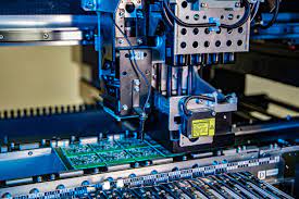
6. Final Assembly: Components and Testing Once the PCB is fabricated, it’s ready for the installation of electronic components. These components can range from tiny surface-mount devices (SMDs) to larger through-hole components. Advanced pick-and-place machines assist in the precise placement of these components, ensuring the integrity of the final product. After assembly, rigorous testing procedures, including automated optical inspection (AOI) and functional testing, confirm that the PCB operates correctly.